Customer Offering
As the world’s largest pure-play MEMS foundry, Silex provides its customers with the industry’s leading MEMS engineering and manufacturing capabilities, enabling them to develop and bring to market the most advanced solutions. Silex has an unparalleled position when it comes to offering the most competitive, capable and unique process technologies to its foundry customers.
To learn more about our wide customer offering;
Get in touch
A Selection of Key Technologies
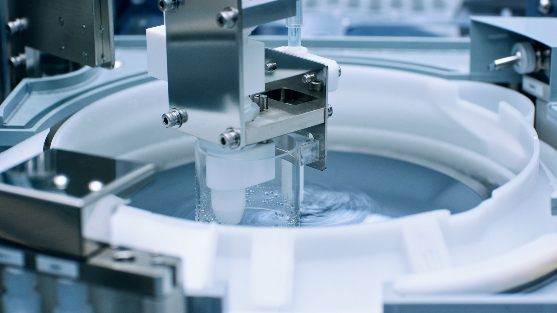
PiezoMEMS
Silex’s commitment to offering Piezoelectric foundry capabilities started well over 15 years ago with the pioneering of a MEMS foundry offer in PiezoMEMS, providing both PZT and AlN processing. Over the last decade, Silex has had a close collaboration with ULVAC in developing the highest performance sputtered PZT and can today offer its foundry customers a fully holistic approach to PZT process integration, with cutting-edge deposition, etch, measurement and analysis capability. Serving innovation leaders, we are receptive to adding novel piezoelectric materials to our foundry offer such as KNN.
Via Technologies
Some of Silex’s early customer products incorporated classical doped poly silicon vias. In 2004, Silex saw its first patented “highly doped silicon” TSV technology (Sil-Via®) integrated by its customer into high volume cell phone application for a 2.5D interposer. This established Silex as a leading provider of through substrate via technologies. Since 2004 we have seen a purpose driven expansion of the portfolio of TSV technologies into metal TSV’s in silicon (Met-Via®), for low resistance applications, and more recently through glass via solutions (TGV) in glass substrates for low parasitics in high voltage and high frequency applications.
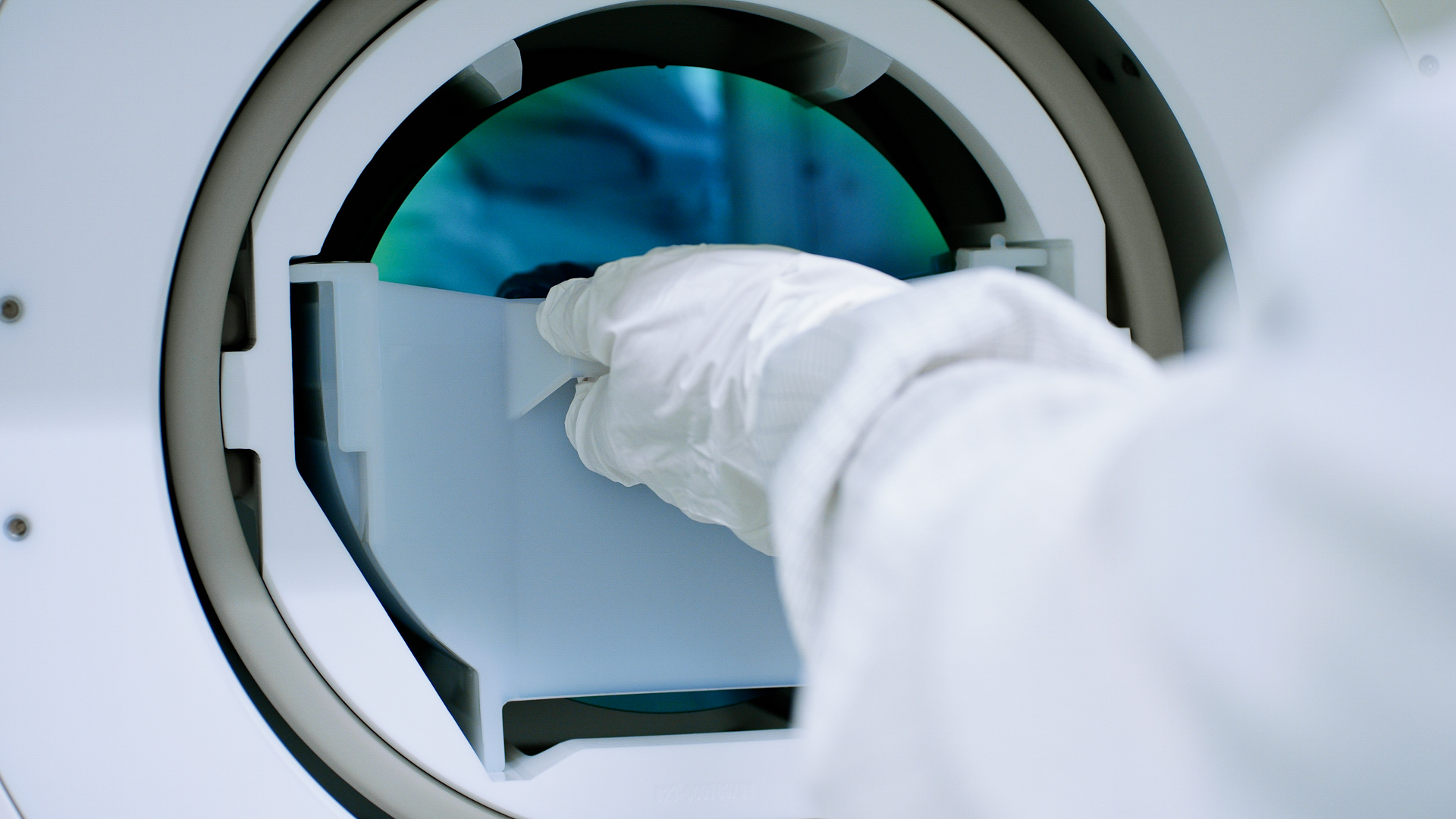
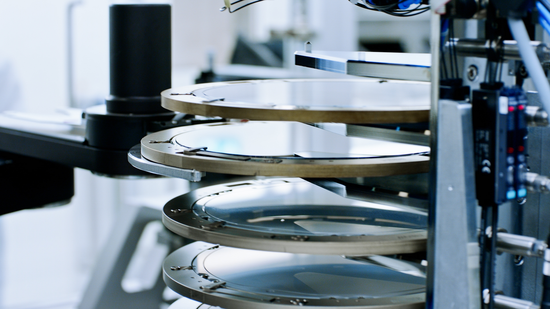
Wafer Level Packaging
Being a leader in the Vias Technology space, combined with our expertise in Deep Reactive Ion Etching (DRIE) and Wafer bonding, provided a natural segway into an WLP offering. Being a MEMS foundry, mastering all aspects of wafer level integration is a must, but at Silex we are constantly pushing the boundaries of what we can provide. MEMS integration is often the most difficult aspect of a full production flow and pushes the foundry to extremes when it comes to available temperature budgets, demands for high precision and accuracy, and processes that can deal with the most demanding topographies and combination of substrates and materials. Silex Bonding capabilities span a wide temperature range and include Direct bonding, Eutectic bonding, Thermocompression bonding, Anodic bonding and Polymer bonding.
Advanced Integration with CMOS and Silicon Photonics
When Silex built the 8” Fab in 2008, we were the first pure-play MEMS foundry to offer a dedicated line for 8” wafer MEMS processing. The main driver for setting up the 8” line was the integration and post-processing on CMOS wafers. We have subsequently seen Silicon Photonics enter as a key driver in the telecom industry for the need to do advanced post processing on wafers coming from a Silicon Photonics foundry. Silex, as a MEMS foundry, has the widest portfolio of capabilities in terms of noble metal processing, AuSn solders, Optical coatings and III-V materials processing that customers may need to differentiate.

Advanced Lithography
At the heart of a Silicon chip is the lithography patterning. In MEMS, the challenge is often not so much about the creation of the smallest feature size, but rather the complex challenge of alignment between layers on different wafers or performing patterning on fully perforated wafers with extreme topographies. Silex has the required toolbox that innovation leaders will need to create the most advanced structures, including full-mass production capacity for laminated dry-films, the widest range of advanced polymers for production, double-sided alignment in our steppers, and spray coating in deep cavities.
Fully Customized MEMS Testing
At Silex we understand the importance for customers in trusting the output from the manufacturing partner. In our manufacturing line we offer the most advanced AOI and analysis equipment available in the market. In addition, we pride ourselves of being a trusted partner to set up fully customized testing of our customers’ devices to be able to deliver 100% fully functional and fully tested Known Good Die (KGD) with respect to any imaginable customer requirement. Our team is capable of setting up advanced die level testing for optical, mechanical, or electrical at a level of complexity that no other MEMS foundry can offer.